Designing the PCB Layout
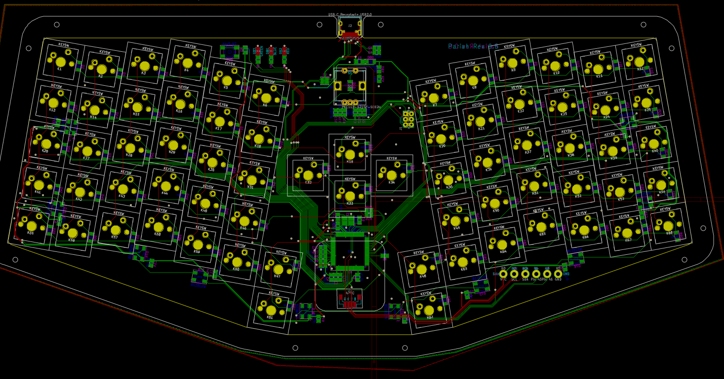
I imported the 2D drawing of the case from Fusion 360 into KiCAD so that I could visually verify the component locations

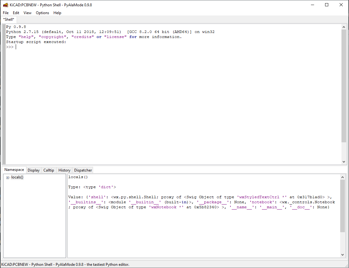
I then began placing the components. Since KiCAD has a Python interface I used that to automate the placement of the keys based on the coordinates from the Fusion sketch.

Once all the keys, and diodes were placed. I then began placing all of the other components. Once the components were placed I drew the traces beginning with the most critical (USB and Crystal) and working my way through all of them. This is an interative process as most of the time I would place a part, draw the traces and then I would figure out a better place and move it an redraw the traces ad nauseum! This process is a bit overwhelming at first, but for me it was best to just dive in and move a trace or a component later rather than try and figure out the optimum placement up-front.

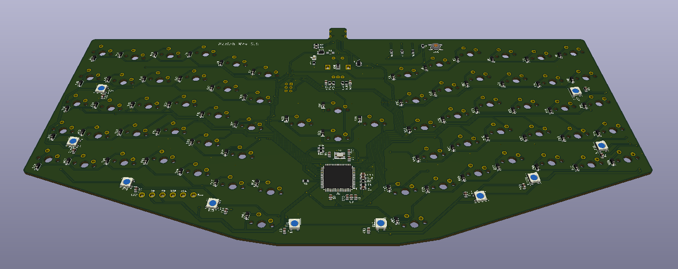
KiCAD includes a pretty neat 3D viewer so that you can get a feel for how the board will look once populated.
